The global semiconductor industry is experiencing rapid growth, driven by digital transformation, Artificial Intelligence (AI), 5G, Electric Vehicles (EVs), and High-Performance Computing (HPC). Key industry trends include:
The global semiconductor market is expected to maintain steady growth. Data centers and HPC will dominate demand, while EVs and smart manufacturing will experience rapid expansion. The demand for industrial automation and smart sensor technologies will also continue to rise.
Semiconductor technologies are fundamental across various sectors, including consumer electronics, industrial automation, automotive electronics, telecommunications, AI/HPC, medical technology, and aerospace & defense. Products such as smartphones, electric vehicles, autonomous driving systems, 5G base stations, AI computing platforms, medical imaging devices, and military radar all heavily rely on semiconductor innovation—driving global industrial advancement and technological upgrading.
Die probing and sorting are critical steps in ensuring product quality and manufacturing efficiency. By identifying defective chips, performing quality grading, and enabling defect repair, manufacturers can lower production costs, improve yield rates, and address diverse market demands—ultimately enhancing overall business outcomes and competitiveness.
By integrating cutting-edge technologies such as machine vision, artificial intelligence (AI), and edge computing, along with multi-axis synchronized control and high-performance hardware, the sorting process can efficiently distinguish between good and defective dies. Manufacturers are continuously optimizing their sorting workflows by adopting real-time data analytics, modular design, and automation to accelerate inspection speed and enhance accuracy. Dies are classified by specification, with out-of-spec units filtered out in early stages, while subsequent sorting steps focus on precise quality categorization—significantly improving yield and production effectiveness.
The reason die sorters need to integrate machine vision and motion control systems is that such combination enables accurate alignment and fast feedback, essential for high-speed and high-precision sorting. The vision system detects die surface quality, position, and dimensions in real time, feeding data to the motion system, which executes accurate multi-axis actions such as pickup, rotation, sorting, and placement. The motion system ensures die stability during high-speed operation, minimizing errors from vibration or misalignment. This reduces the sorting cycle, limits manual intervention, and increases both productivity and reliability—ultimately meeting evolving market needs.

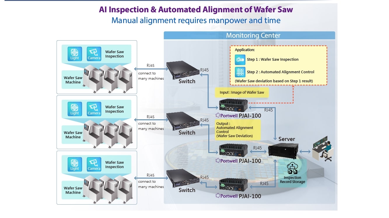
Edge AI systems offer intelligent inspection solutions for wafer dicing by addressing the limitations of manual alignment and improving positional accuracy through AI-based automation. This technology strikes a balance between operational efficiency and reduced labor dependency. In a typical use case, an industrial camera captures images of the dicing position under controlled lighting. These images are transmitted from the wafer saw machine to the edge AI system via a network switch. The AI system analyzes and compares the image data to verify whether the cutting position is aligned. If misalignment is detected, the AI system automatically initiates a calibration procedure, instructing the dicing machine to perform precise corrections.

The fanless compact PJAI-100-ON edge AI system is ideal for semiconductor wafer dicing inspection and automated calibration. It is powered by the NVIDIA® Jetson Orin Nano™ SOM, which enables fast and accurate detection of dicing misalignments.
Equipped with 4GB/8GB of LPDDR5 memory, the system ensures rapid image processing and multitasking performance, including real-time inspection and calibration control.
Includes an M.2 slot for NVMe storage, which significantly improves data throughput. It also features dual RJ45 GbE ports to facilitate high-speed connections between network switches and servers—simultaneously supporting image transmission, dicing correction control, and data backup.
Offers USB and COM ports for integration with other peripheral devices and machine components.
In this application architecture, three PJAI-100-ON edge AI systems are deployed. Each unit connects to multiple wafer dicing machines via a network switch, enabling centralized AI-based inspection and automated calibration, resulting in a more precise and efficient dicing process.
As semiconductor processes continue to advance, IC die bonding has become an increasingly critical stage in the back-end packaging process. This step requires extremely high precision to attach the die onto the package substrate, directly influencing the performance and reliability of semiconductor devices. As such, the die bonder is considered one of the most vital pieces of equipment in the packaging and testing segment.
The die bonder picks up individual chips from diced wafers and accurately places them onto substrates. The bonding is typically performed using silver epoxy, ensuring firm adhesion between the chip and the substrate. To meet the demands of modern semiconductor packaging, die bonders must support high-speed, high-precision operations, including alignment, flipping, and continuous placement. As bonding accuracy standards become increasingly stringent, traditional optical inspection methods can no longer meet micron-level precision and stability requirements. Therefore, the adoption of automated precision die bonders has become essential—not only improving yield and efficiency, but also minimizing human error and enhancing process stability.
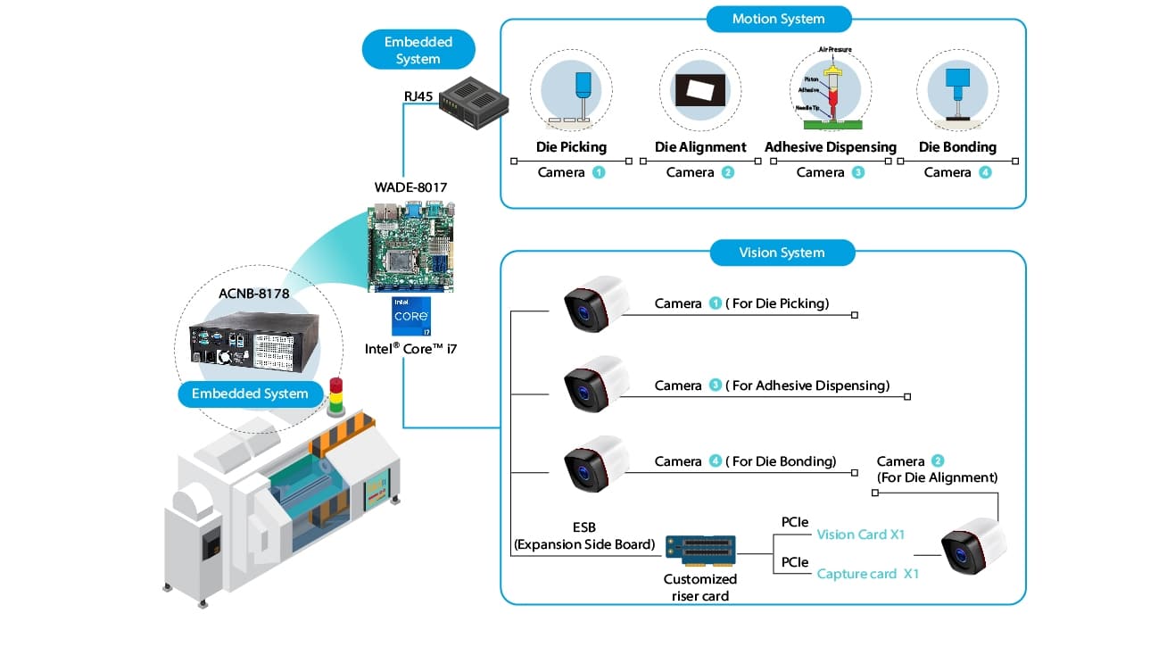
During the IC die bonding process, the motion system and vision inspection system inside the bonder work in tandem to perform ultra-fast and highly accurate die alignment. The vision system is responsible for real-time detection of the die’s position and angle. It uses image processing algorithms to calculate the relative position between the die and the substrate and provides compensation data. The motion system then dynamically adjusts its actions based on this data to ensure precise pickup and placement. This synchronization avoids cumulative errors and keeps bonding deviation within the micron (μm) range.
Insufficient bonding precision can result in electrical misalignment or degraded thermal conductivity, directly affecting product performance and even the success of the packaging production line. Thus, the coordinated operation between the vision system (providing real-time calibration data) and the motion system (executing high-speed, accurate adjustments) is essential to building high-precision die bonding equipment.

Portwell’s custom solution, featuring the WADE-8017 Mini-ITX form factor motherboard, supports 6th and 7th Gen Intel® Core™ i3/i5/i7 processors, providing the computational power required for high-resolution image capture and die position detection.
The system’s DDR4 memory allows for fast analysis of alignment markers on substrates and enables rapid execution of compensation calculations. This ensures the motion system can precisely guide the die placement operation, improving bonding accuracy and throughput.
Portwell is recognized for its technological innovation and high-quality products, delivering solutions that ensure reliability, durability, and outstanding performance to meet the demands of advanced technologies and harsh environments in the semiconductor industry.
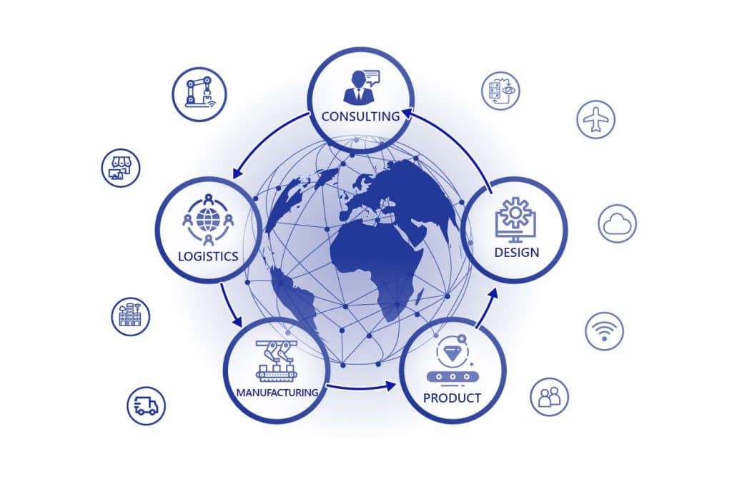
Portwell’s Design and Manufacturing Services (DMS) offer end-to-end, fully customized support for semiconductor applications—from product design to production and global logistics. These services enable customers to rapidly transform innovative concepts into reality while ensuring long-term and stable product availability, a critical requirement in the fast-evolving semiconductor market.

Portwell products are widely deployed in mission-critical industrial environments, including automation, medical equipment and railway systems. The company’s solutions demonstrate exceptional stability, precision and reliability, making them especially well-suited for semiconductor applications that demand uncompromising performance and dependability.
Portwell’s global footprint further enhances its ability to support customers with localized technical service and rapid response in key regions such as Taiwan, the United States, Japan, China, the United Kingdom, Germany, and India. This worldwide support network ensures that Portwell can efficiently address the diverse requirements of semiconductor clients across regions, consistently creating value for its partners.
As a leading provider of edge computing and industrial computer solutions, Portwell not only stays ahead of technology trends but also leverages its extensive DMS expertise to become a trusted partner in the semiconductor domain. Looking ahead, Portwell will continue to place innovation at the core of its strategy, delivering cutting-edge, high-performance solutions that empower customers to surmount technical challenges and drive sustainable growth.